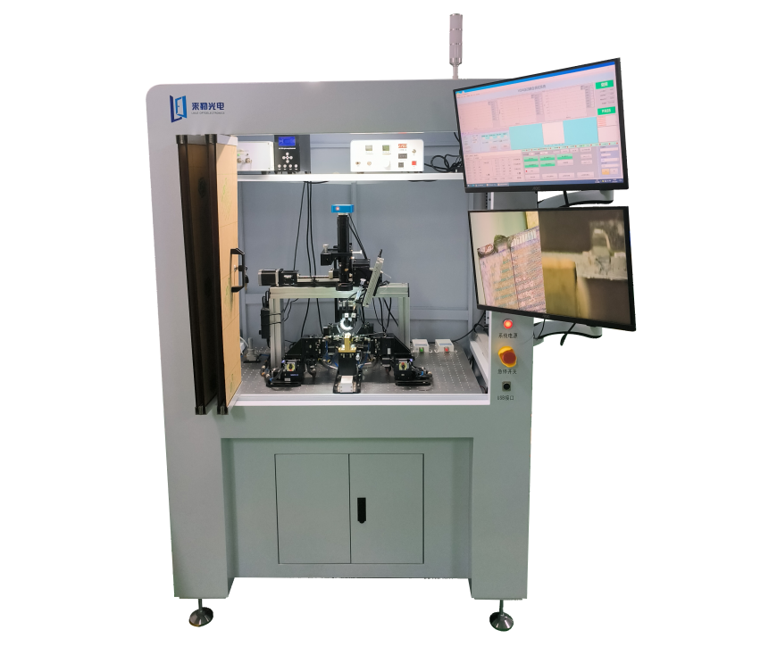
Silicon Photonic Chip Automatic Coupling Test System
Product Features
Automatic pick-up from wafer blue film, with automatic inspection and sorting, adaptable to different wafer sizes;
Fast chip loading and unloading with automatic material handling;
Compatible with both horizontal and vertical coupling; automatic alignment and coupling between chip and input/output FAs, with single coupling cycle time of < 3 seconds;
Automatic light seeking, FA-to-chip gap control (accuracy ±5μm), and multi-channel balancing;
Automatic power-on with probe arrays precisely contacting chip pad arrays; supports individual channel power-on as well as simultaneous power-on for all channels;
Compatible with both horizontal and vertical coupling, with expandable upgrade for 8-inch wafer testing.
The Silicon Photonic Chip Fully Automatic Coupling Test System is capable of simultaneously meeting both chip coupling and testing requirements. The system supports coupling and testing for various types of chips, bars, and wafers. It features flexible parameter configuration, a visual user interface, and user-friendly operation. This equipment is suitable for coupling and testing of a wide range of materials, including silicon photonics, thin-film lithium niobate, and III-V compound semiconductors.
Product Features
Automatic pick-up from wafer blue film, with automatic inspection and sorting, adaptable to different wafer sizes;
Fast chip loading and unloading with automatic material handling;
Compatible with both horizontal and vertical coupling; automatic alignment and coupling between chip and input/output FAs, with single coupling cycle time of < 3 seconds;
Automatic light seeking, FA-to-chip gap control (accuracy ±5μm), and multi-channel balancing;
Automatic power-on with probe arrays precisely contacting chip pad arrays; supports individual channel power-on as well as simultaneous power-on for all channels;
Compatible with both horizontal and vertical coupling, with expandable upgrade for 8-inch wafer testing.